Transient absorption spectroscopy and 2D semiconductors
2D-Semiconductors
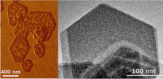


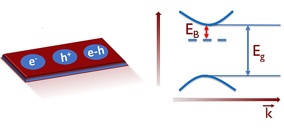


Using wet-chemical synthesis methods associated to the ones applied for 0D nanocrystals, we obtain 2D semiconductors with a thickness of mono- or few-layers. By guiding the reaction via surface ligands and growth control, anisotropic ultrathin 2D layers of typically isotropically crystallizing semiconductor systems synthesized that are not accessible by exfoliation methods.
Depending on their lateral size, the so-called nanosheets or nanoplatelets have intriguing optoelectronic properties that are caused by their strong size quantization in one dimension, their thickness.
E.g. under photoexcitation, strongly bound electron-hole pairs, so-called excitons, are generated in nanosheets and nanoplatelets, which can emit light of a certain wavelength when recombining and have high potential for light-emitting diodes or even lasing. Furthermore, highly mobile free charge carriers can be photogenerated, which are needed for fast switching transistors, photodetectors or solar cells.
We obtain colloidal 2D semiconductor inks that can be processed easily onto different surfaces, substrates and cover the UV-Vis region up to the NIR/SWIR in terms of absorption and emission.
Transient Absorption Spectroscopy
EN [Spalten: Transiente Absorptions-Spektroskopie I]
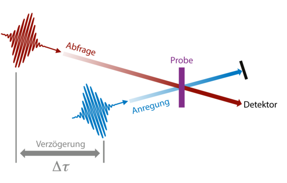


Transient absorption spectroscopy (TAS) allows for the comprehensive investigation of the nature, origin and dynamics of photoexcited charge carriers in optically active systems. In TAS, samples get photoexcited from the ground state to the excited state with ultrashort laser pulses (~100 fs), which allow studying the sample response while relaxing at different points after photoexcitation via time-delayed probe pulses.
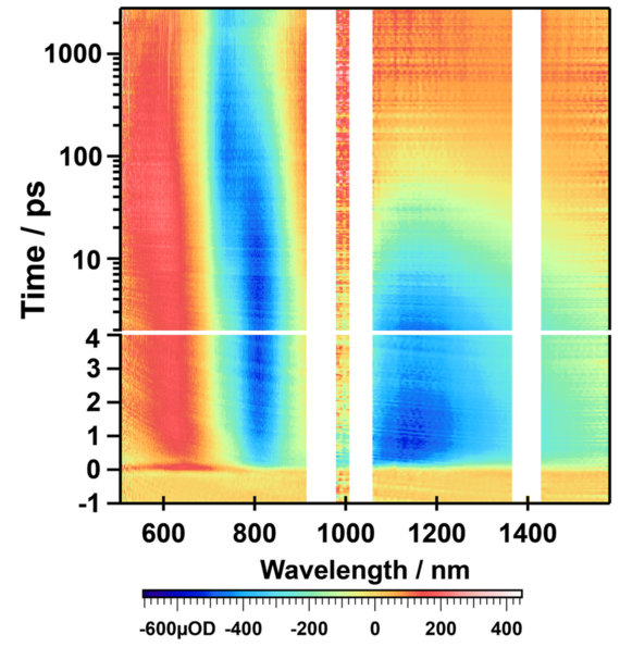


With this method, short-lived recombination dynamics of the charge carriers can be character ized in real time (0.5 ps to 8 ns) over a spectroscopic broadband range of 350 nm to (currently) 1600 nm. TAS differs from time-resolved photoluminescence spectroscopy such that it allows tracing of so-called dark states, which are not accessible via photoluminescence. We use TAS to characterize the optoelectronic properties of ultrathin 2D semiconductors as well as 0D semiconductor nanocrystals, plasmonic nanocrystals, nanocrystal assemblies and hybrid structures.
EN [Spalten: Transiente Absorptions-Spektroskopie III]
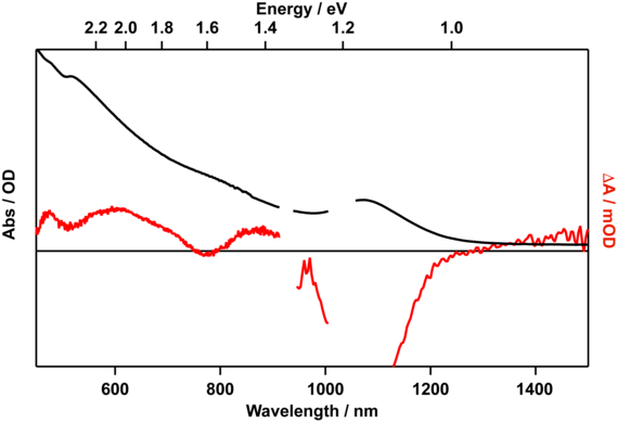


The broadband TA spectrometer is operated by the Department for Functional Nanostructures (Lauth/Bigall/Dorfs) in collaboration with the group of Prof. M. Oestreich and Dr. J. Hübner (femtosecond laser amplifier system) at the Institute of Solid State Physics.
Institutional Embedding
EN [Bildkarte: Professur]


30167 Hannover


